2018-03-04
The Swiss Mechatronic Art Society (SGMK) and ANORG hosted a KitSprint in Zurich last weekend which was an effort to bring the local electronics community together, encourage people to document existing electronics kit ideas, create new ones and put them all up on Kitspace. This was also part of the closing down celebrations of the ANORG Atelier that has been, for almost a decade, a co-working/co-living space for artists, architects, musicians, bio and electronics hackers — pretty much anyone with an artistic bent and a desire to create.
A group of about 15 electronics geeks descended on the ANORG space. Our energy was focused on meeting, talking with each other, eating and drinking together, soldering (my jellyfish bristle-bot kit was popular with adults and kids alike), but also getting things “Shenzhen Ready!” a phrase coined by Marc Dusseiller, the event’s main organizer, for getting your design into a state to be fabricated — most likely through an order from Shenzhen, China. Calls for making it “Shenzhen Ready!” and to “send it off to China!” would frequently echo the halls interspersed with the noise of the tesla coil Chris Vernon had set up and Heinzme’s experiments with explosives. Some funding was provided by Migros Kulturprozent for travel costs, food and drinks but also to cover the cost of ordering PCBs for those that had brought their projects into a Shenzhen Ready state by Sunday evening.
The SGMK community had originally been founded by a group of DIY synthesizer geeks so noise makers featured prominently in the projects that were chosen. Oli Jäggi chose to re-make a circuit dubbed the Solar Bird which had been the first project he etched and soldered after joining the SGMK. This little oscillator is completely solar powered and gives out a cricket-like chirp when it is given enough light. His idea was to take a known working circuit but give it a more interesting and pleasant shape.

images: Left and middle, CC-BY-SA, tamberg. Right, Andreas Kopp.
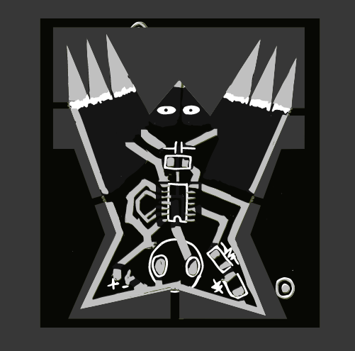
Oli’s method consists of drawing traces by hand to scale, scanning this and printing onto a transparency and then etching it. For the Shenzhen ready version he converted to Gerber by use of KiCad’s Bitmap2Component tool. A similar more approachable method, but maybe more laboursome on the part of a workshop instructor, has been developed by Marc. Something he calls DIY CAD (Do It Yourself Children Aided Design) where component footprints are prepared as laminated paper drawings in a scaled up form. People are instructed to draw the outline and tracks of their circuit layout, using pencil on paper first and then then markers on projector transparencies. The drawings are scanned, scaled-down, exposed and then etched onto copper clad boards.

image: Andreas Kopp
I took two runs at this process and felt I had good success on my second run where I managed to layout a squeaking Maulwurf (German for mole) from a battery-powered tri nand gate oscillator schematic Marc had provided. I am very happy with the result as it fits neatly into your hand but it also feels natural to stick into a plant pot and leave it there where it will squeak and blink depending on the soil moisture.


On the whole the community seems to enjoy pushing the boundaries of what the copper plated fiber glass allows. This is paired with a cultivated and shared skill of home-etching which allows you to hold a board in your hands almost immediately after designing it. Some folks at SGMK have even been experimenting with a coating solution which allowed me to make the tips of the mole’s paws silver.
Home etching is slowly becoming a bit of a lost art in the electronics hobbyist community with PCB batching services for industrial fabrication now being extremely affordable. The immediate feedback and the intution it gives you for the manufacturing process still make it a must for any PCB designer to try though. Using alternative approaches to layout, such as the DIY CAD method, make it a much more fun, artistic process that is a far cry from the frustrations of using your typical CAD PCB layout tool.
But at SGMK there is also much excitement for exploring what can be done with the added layers and processes that come with industrial manufacture and this event was about sending them off to China after all! When transferring these designs to the Gerber format required by the manufacturers, an oft repeated feature is to free all traces of the solder mask which gives the board a home-etched look and contrasts nicely with the solder mask colours in the surrounding space.

NeoCoco Cat PCB: Tuomo Tamenpää, co-designed with Marc Dusseiller in Taipei (Re-design of the 8Bit Mixtape)
Unagi (Fish) PCB: Masato Takemura, Take-Space, Fablab Hamamatsu
When making my Maulwurf design Shenzhen Ready (!) I chose to expose most of the tracks but keep the solder mask in places where it would make it easier to solder. I also drew the mask, back copper and the front silkscreen with the DIY CAD method. Drawing some fiduciary markers helped to align all the layers in post processing but of course the alignment is still a little rough.

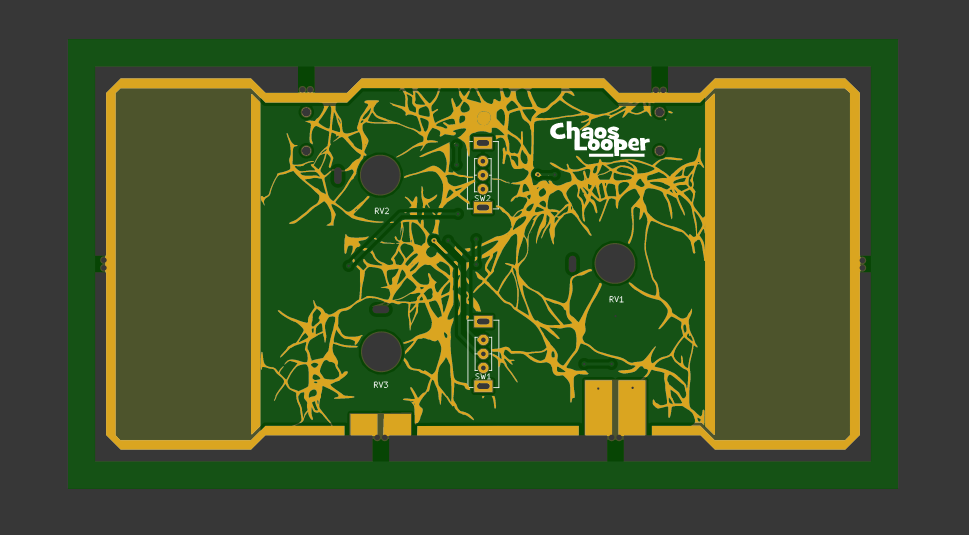
Urs Gaudenz chose to “productize” a circuit he had built up in several hand-made versions already: the Chaos Looper. Here an older delay chip is tortured into making new and interesting sounds through adjustment of feedback loops. This design is a more mainstream approach: schematic and layout was done in KiCad. The look and feel though was physically mocked up and one side of the PCB copper layer was drafted on paper, with a neuron inspired graphic, as well. Bringing these more creative elements onto the circuit board makes this design stand out and feel complete without an external case.

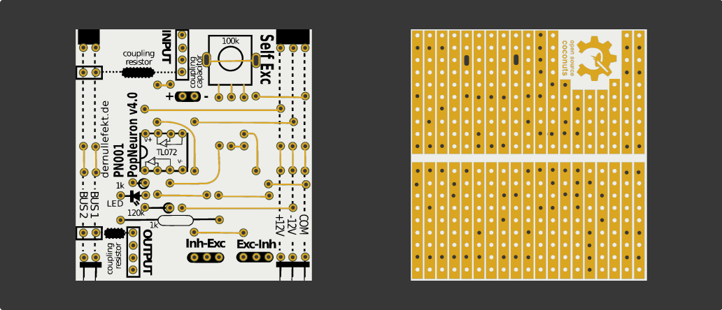
Marc took on the task of making some other people’s designs Shenzhen Ready (!) while also experimenting with some new class-D amplifier circuits. One of the most striking results is the Shenzhen Ready version of Wolfgang Spahn’s Pop Neuron, an analog neuron simulation. These are usually completely hand-soldered onto prototyping boards during Wolfgang’s workshops. Marc turned the graphic, that is normally printed on paper as a wiring guide, into actual connections on the top copper layers. On the bottom copper we have the typical connections of a prototyping board. Wolfgang joined via video chat as well to better explain the functioning of these circuits and their design.

Properly documenting the bill of materials for these projects, so people anywhere in the world can better replicate them, is often still an after thought. In the days leading up the event I pushed myself to put up an alpha version of my BOM builder tool that could help people with this task. I received good feedback as people started to make use of it though this version can only download/upload BOMs in the Kitspace “native” 1-click BOM TSV format. Over the coming months I plan to expand this and integrate it into Kitspace proper and hopefully the designers will take the time to document these amazing creations in full.
